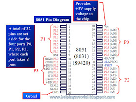
I/O Programming
- The four 8-bit I/O ports P0, P1, P2 and P3 each uses 8 pins
- All the ports upon RESET are configured as input, ready to be used as input ports
- When the first 0 is written to a port, it becomes an output
- To reconfigure it as an input, a 1 must be sent to the port
- To use any of these ports as an input port, it must be programmed
Why P0 Need Pull Up Resistor?
P0 is open drain, so each pin of P0 must be connected externally to a 10K ohm pull up resistor.
- Open drain is a term used ofr MOC chips in the same way that open collector is use for TTL chips.
Example:
- The following code will continuously send out to port 0 the alternating value 55H and AAH
BACK:
MOV A,#55H
MOV P0,A
ACALL DELAY
MOV A,#0AAH
MOV P0,A
ACALL DELAY
SJMP BACK
Example:
Port 0 is configured first as an input port by writing 1s to it, and then data is received from that port and sent to P1
MOV A,#0FFH ;A=FF hex
MOV P0,A ;make P0 an i/p port
;by writing it all 1s
BACK:
MOV A,P0 ;get data from P0
MOV P1,A ;send it to port 1
SJMP BACK ;keep doing it
Example:
Port 1 is configured first as an input port by writing 1s to it, then data is received from that port and saved in R7 and R5
MOV A,#0FFH ;A=FF hex
MOV P1,A ;make P1 an input port
;by writing it all 1s
MOV A,P1 ;get data from P1
MOV R7,A ;save it to in reg R7
ACALL DELAY ;wait
MOV A,P1 ;another data from P1
MOV R5,A ;save it to in reg R5
Additional Functions of Port 3
Port 3 has the additional function of providing some extremely important signals
Complete Program Example
- Write a program to toggle all the bits of P0, P1, and P2 every 1/4 of a second
ORG 0
BACK:
MOV A,#55H
MOV P0,A
MOV P1,A
MOV P2,A
ACALL QSDELAY ;Quarter of a second
MOV A,#0AAH
MOV P0,A
MOV P1,A
MOV P2,A
ACALL QSDELAY
SJMP BACK
QSDELAY:
MOV R5,#11
H3: MOV R4,#248
H2: MOV R3,#255
H1: DJNZ R3,H1 ;4 MC for DS89C4x0
DJNZ R4,H2
DJNZ R5,H3
RET
END
Delay Calculation
= 11 × 248 × 255 × 4 MC × 90 ns
= 250,430 μs
The entire 8 bits of Port 1 are accessed
BACK:
MOV A,#55H
MOV P1,A
ACALL DELAY
MOV A,#0AAH
MOV P1,A
ACALL DELAY
SJMP BACK
Rewrite the code in a more efficient manner by accessing the port directly without going through the accumulator
BACK:
MOV P1,#55H
ACALL DELAY
MOV P1,#0AAH
ACALL DELAY
SJMP BACK
Another way of doing the same thing
MOV A,#55H
BACK:
MOV P1,A
ACALL DELAY
CPL A
SJMP BACK
Bit Addressing of Port:
- Sometimes we need to access only 1 or 2 bits of the port
Example:
BACK:
CPL P1.2 ;complement P1.2
ACALL DELAY
SJMP BACK
;another variation of the above program
AGAIN:
SETB P1.2 ;set only P1.2
ACALL DELAY
CLR P1.2 ;clear only P1.2
ACALL DELAY
SJMP AGAIN
Write the following programs.
- Create a square wave of 50% duty cycle on bit 0 of port 1.
Solution:
- The 50% duty cycle means that the “on” and “off” state (or the high and low portion of the pulse) have the same length. Therefore, we toggle P1.0 with a time delay in between each state.
HERE:
SETB P1.0 ;set to high bit 0 of port 1
LCALL DELAY ;call the delay subroutine
CLR P1.0 ;P1.0=0
LCALL DELAY
SJMP HERE ;keep doing it
Another way to write the above program is:
HERE:
CPL P1.0 ;set to high bit 0 of port 1
LCALL DELAY ;call the delay subroutine
SJMP HERE ;keep doing it
Example:
Write a program to perform the following:
- Keep monitoring the P1.2 bit until it becomes high
- When P1.2 becomes high, write value 45H to port 0
- Send a high-to-low (H-to-L) pulse to P2.3
Solution:
SETB P1.2 ;make P1.2 an input
MOV A,#45H ;A=45H
AGAIN:
JNB P1.2,AGAIN ; get out when P1.2=1
MOV P0,A ;issue A to P0
SETB P2.3 ;make P2.3 high
CLR P2.3 ;make P2.3 low for H-to-L
Example:
Assume that bit P2.3 is an input and represents the condition of an oven. If it goes high, it means that the oven is hot. Monitor the bit continuously. Whenever it goes high, send a high-to-low pulse to port P1.5 to turn on a buzzer.
Solution:
HERE:
JNB P2.3,HERE ;keep monitoring for high
SETB P1.5 ;set bit P1.5=1
CLR P1.5 ;make high-to-low
SJMP HERE ;keep repeating
Example:
A switch is connected to pin P1.7. Write a program to check the status of SW and perform the following:
- If SW=0, send letter ‘N’ to P2
- If SW=1, send letter ‘Y’ to P2
Solution:
SETB P1.7 ;make P1.7 an input
AGAIN:
JB P1.2,OVER ;jump if P1.7=1
MOV P2,#’N’ ;SW=0, issue ‘N’ to P2
SJMP AGAIN ;keep monitoring
OVER:
MOV P2,#’Y’ ;SW=1, issue ‘Y’ to P2
SJMP AGAIN ;keep monitoring
Example:
A switch is connected to pin P1.7. Write a program to check the status of SW and perform the following:
- If SW=0, send letter ‘N’ to P2
- If SW=1, send letter ‘Y’ to P2
Use the carry flag to check the switch status.
Solution:
SETB P1.7 ;make P1.7 an input
AGAIN:
MOV C,P1.2 ;read SW status into CF
JC OVER ;jump if SW=1
MOV P2,#’N’ ;SW=0, issue ‘N’ to P2
SJMP AGAIN ;keep monitoring
OVER:
MOV P2,#’Y’ ;SW=1, issue ‘Y’ to P2
SJMP AGAIN ;keep monitoring


please tell me how to interface 8952 using dev board
ReplyDelete